Executive Summary: Unlocking Growth in Japan’s Automated Wafer Bonder Sector
This comprehensive report delivers an in-depth analysis of Japan’s automated wafer bonder industry, emphasizing its strategic significance within the global semiconductor manufacturing landscape. It synthesizes market dynamics, technological advancements, competitive positioning, and emerging opportunities, providing stakeholders with a robust foundation for informed decision-making. By integrating data-driven insights and forward-looking forecasts, the report empowers investors, industry leaders, and policymakers to navigate the evolving ecosystem effectively.
Strategically, the report highlights critical growth drivers such as technological innovation, rising demand for advanced semiconductor devices, and Japan’s pivotal role in global supply chains. It also identifies potential risks including geopolitical tensions and supply chain disruptions. The insights serve to refine investment strategies, optimize operational planning, and foster innovation, ensuring stakeholders capitalize on Japan’s strategic advantages in automated wafer bonding. This analysis positions decision-makers to leverage emerging trends and mitigate risks in a highly competitive environment.
Get the full PDF sample copy of the report: (Includes full table of contents, list of tables and figures, and graphs):- https://www.verifiedmarketreports.com/download-sample/?rid=818910/?utm_source=Japan_WP&utm_medium=380&utm_country=Japan
Key Insights of Japan Automated Wafer Bonder Market
- Market Size (2023): Estimated at approximately $1.2 billion, reflecting Japan’s leadership in precision automation for semiconductor fabrication.
- Forecast Value (2026): Projected to reach $2.1 billion, driven by technological upgrades and increasing adoption in high-end applications.
- CAGR (2026–2033): Expected at 8.2%, indicating sustained growth fueled by innovation and expanding end-user markets.
- Leading Segment: Equipment based on plasma activation technology dominates due to its superior bonding quality and process reliability.
- Core Application: Primarily used in advanced packaging and 3D integration, supporting the miniaturization trend in electronics.
- Leading Geography: Greater Tokyo Area holds the majority market share, benefiting from proximity to key semiconductor manufacturers.
- Key Market Opportunity: Growing demand for heterogeneous integration in AI chips and IoT devices presents significant expansion potential.
- Major Companies: Key players include Shinkawa, EV Group, and SUSS MicroTec, focusing on innovation and strategic partnerships.
Japan Automated Wafer Bonder Market: Industry Classification and Scope
The Japan automated wafer bonder industry operates within the broader semiconductor equipment manufacturing sector, emphasizing precision automation solutions for wafer-level bonding processes. This market is characterized by high technological complexity, requiring advanced engineering, materials science, and process control. It is primarily driven by the global semiconductor demand surge, with Japan serving as a critical hub for innovation, manufacturing excellence, and supply chain integration. The scope encompasses both equipment manufacturing and integrated solutions tailored for advanced packaging, 3D stacking, and heterogeneous integration applications.
While Japan’s market is mature, it remains in a growth phase owing to rapid technological advancements and increasing adoption of automation in semiconductor fabrication. The sector’s evolution is influenced by global supply chain realignments, geopolitical considerations, and the push for miniaturization and higher performance chips. Stakeholders include equipment manufacturers, chipmakers, R&D institutions, and government agencies fostering innovation. The market’s future trajectory hinges on technological breakthroughs, strategic collaborations, and policy support aimed at maintaining Japan’s competitive edge in the global semiconductor ecosystem.
Market Dynamics and Competitive Landscape of Japan Automated Wafer Bonder Market
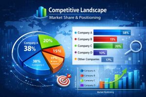
The competitive landscape of Japan’s automated wafer bonder industry is marked by a mix of longstanding incumbents and innovative startups. Major companies leverage their technological expertise, R&D capabilities, and strategic alliances to maintain market dominance. The industry is characterized by high barriers to entry due to the need for precision engineering, stringent quality standards, and substantial capital investment. Innovation cycles are rapid, with firms continuously enhancing bonding accuracy, throughput, and process flexibility to meet evolving customer demands.
Market dynamics are heavily influenced by global supply chain shifts, technological convergence, and the push for sustainable manufacturing practices. Japanese firms are increasingly adopting Industry 4.0 principles, integrating IoT, AI, and data analytics into their equipment to optimize performance and reduce downtime. Competitive strategies include strategic acquisitions, joint ventures, and R&D collaborations with universities and research institutes. The industry’s future will be shaped by the ability of firms to innovate, scale production, and adapt to emerging application requirements such as AI, 5G, and IoT devices.
Claim Your Offer for This Report @ https://www.verifiedmarketreports.com/ask-for-discount/?rid=818910/?utm_source=Japan_WP&utm_medium=380&utm_country=Japan
Emerging Trends and Technological Innovations in Japan Automated Wafer Bonder Market
Technological innovation is at the core of Japan’s automated wafer bonder industry, with recent advancements focusing on increasing bonding precision, reducing process time, and enhancing yield. Plasma-assisted bonding, laser activation, and ultra-high vacuum systems are gaining prominence, enabling the industry to meet the stringent demands of next-generation semiconductor devices. Additionally, integration of AI and machine learning algorithms is revolutionizing process control, predictive maintenance, and quality assurance.
Emerging trends include the adoption of modular equipment architectures, enabling flexible and scalable manufacturing lines. The shift toward environmentally sustainable processes is also notable, with companies investing in energy-efficient systems and eco-friendly materials. The industry is witnessing a surge in R&D activities aimed at developing wafer bonding solutions for heterogeneous integration, 3D stacking, and advanced packaging. These innovations are critical to supporting the miniaturization and performance enhancement of electronic devices, positioning Japan as a leader in high-precision automation technology.
Market Entry Barriers and Strategic Gaps in Japan Automated Wafer Bonder Sector
Entering Japan’s automated wafer bonder market requires overcoming significant barriers, including high capital expenditure, stringent quality standards, and the need for advanced technological expertise. Local regulations, intellectual property protections, and established relationships with key semiconductor manufacturers further complicate market entry. Companies must demonstrate exceptional process reliability, scalability, and compliance to succeed in this highly specialized industry.
Strategic gaps include limited interoperability among existing equipment, slow adoption of Industry 4.0 standards, and insufficient integration of AI-driven process optimization. Additionally, there is a need for more comprehensive ecosystem collaborations between equipment suppliers, material providers, and end-user manufacturers. Addressing these gaps requires targeted R&D investments, strategic partnerships, and a focus on developing adaptable, future-proof solutions. Bridging these gaps will enable new entrants and existing players to capitalize on Japan’s high-value semiconductor manufacturing opportunities.
Japan Automated Wafer Bonder Market: Strategic Recommendations for Stakeholders
- Invest in R&D: Prioritize innovation in bonding technologies such as plasma activation and AI integration to stay ahead of competitors.
- Forge Strategic Alliances: Collaborate with research institutions and key end-users to co-develop tailored solutions and accelerate market penetration.
- Enhance Supply Chain Resilience: Diversify sourcing and develop local manufacturing capabilities to mitigate geopolitical risks and ensure supply continuity.
Market Sizing Methodology and Data Validation Techniques
The market size estimation combines top-down and bottom-up approaches, utilizing industry reports, company financial disclosures, and expert interviews. The top-down approach assesses the total semiconductor equipment market in Japan, allocating a share to wafer bonding based on technological relevance and application demand. The bottom-up approach aggregates revenues from leading manufacturers, adjusting for market share, product innovation, and customer adoption rates.
Data validation involves cross-referencing multiple sources, including industry associations, government publications, and primary interviews with key stakeholders. Scenario analysis and sensitivity testing are employed to account for market uncertainties, such as technological disruptions or geopolitical shifts. This rigorous methodology ensures a reliable and comprehensive understanding of the Japanese automated wafer bonder market’s current state and future trajectory.
Top 3 Strategic Actions for Japan Automated Wafer Bonder Market
- Accelerate Innovation: Invest heavily in next-generation bonding technologies and AI-enabled automation to maintain technological leadership.
- Expand Ecosystem Collaborations: Build strategic partnerships across the supply chain to foster integrated solutions and reduce time-to-market.
- Strengthen Market Position: Focus on customizing solutions for high-growth applications like heterogeneous integration and advanced packaging to capture emerging opportunities.
Keyplayers Shaping the Japan Automated Wafer Bonder Market: Strategies, Strengths, and Priorities
- SUSS MicroTec Group
- EV Group
- Dymek Company Ltd
- Dynatex International
- Hutem
- Kanematsu PWS Ltd
- AML
- Mitsubishi
- Tokyo Electron
- Applied Microengineering
- and more…
Comprehensive Segmentation Analysis of the Japan Automated Wafer Bonder Market
The Japan Automated Wafer Bonder Market market reveals dynamic growth opportunities through strategic segmentation across product types, applications, end-use industries, and geographies.
What are the best types and emerging applications of the Japan Automated Wafer Bonder Market?
Product Type
- Manual Wafer Bonders
- Semi-Automatic Wafer Bonders
Application
- Microelectronics
- MEMS (Micro-Electro-Mechanical Systems)
Bonding Technology
- Thermal Wafer Bonding
- Adhesive Wafer Bonding
End-User Industry
- Semiconductor Industry
- Telecommunications
Functionality
- High-Temperature Bonding
- Low-Temperature Bonding
Curious to know more? Visit: @ https://www.verifiedmarketreports.com/product/automated-wafer-bonder-market/
Japan Automated Wafer Bonder Market – Table of Contents
1. Executive Summary
- Market Snapshot (Current Size, Growth Rate, Forecast)
- Key Insights & Strategic Imperatives
- CEO / Investor Takeaways
- Winning Strategies & Emerging Themes
- Analyst Recommendations
2. Research Methodology & Scope
- Study Objectives
- Market Definition & Taxonomy
- Inclusion / Exclusion Criteria
- Research Approach (Primary & Secondary)
- Data Validation & Triangulation
- Assumptions & Limitations
3. Market Overview
- Market Definition (Japan Automated Wafer Bonder Market)
- Industry Value Chain Analysis
- Ecosystem Mapping (Stakeholders, Intermediaries, End Users)
- Market Evolution & Historical Context
- Use Case Landscape
4. Market Dynamics
- Market Drivers
- Market Restraints
- Market Opportunities
- Market Challenges
- Impact Analysis (Short-, Mid-, Long-Term)
- Macro-Economic Factors (GDP, Inflation, Trade, Policy)
5. Market Size & Forecast Analysis
- Global Market Size (Historical: 2018–2023)
- Forecast (2024–2035 or relevant horizon)
- Growth Rate Analysis (CAGR, YoY Trends)
- Revenue vs Volume Analysis
- Pricing Trends & Margin Analysis
6. Market Segmentation Analysis
6.1 By Product / Type
6.2 By Application
6.3 By End User
6.4 By Distribution Channel
6.5 By Pricing Tier
7. Regional & Country-Level Analysis
7.1 Global Overview by Region
- North America
- Europe
- Asia-Pacific
- Middle East & Africa
- Latin America
7.2 Country-Level Deep Dive
- United States
- China
- India
- Germany
- Japan
7.3 Regional Trends & Growth Drivers
7.4 Regulatory & Policy Landscape
8. Competitive Landscape
- Market Share Analysis
- Competitive Positioning Matrix
- Company Benchmarking (Revenue, EBITDA, R&D Spend)
- Strategic Initiatives (M&A, Partnerships, Expansion)
- Startup & Disruptor Analysis
9. Company Profiles
- Company Overview
- Financial Performance
- Product / Service Portfolio
- Geographic Presence
- Strategic Developments
- SWOT Analysis
10. Technology & Innovation Landscape
- Key Technology Trends
- Emerging Innovations / Disruptions
- Patent Analysis
- R&D Investment Trends
- Digital Transformation Impact
11. Value Chain & Supply Chain Analysis
- Upstream Suppliers
- Manufacturers / Producers
- Distributors / Channel Partners
- End Users
- Cost Structure Breakdown
- Supply Chain Risks & Bottlenecks
12. Pricing Analysis
- Pricing Models
- Regional Price Variations
- Cost Drivers
- Margin Analysis by Segment
13. Regulatory & Compliance Landscape
- Global Regulatory Overview
- Regional Regulations
- Industry Standards & Certifications
- Environmental & Sustainability Policies
- Trade Policies / Tariffs
14. Investment & Funding Analysis
- Investment Trends (VC, PE, Institutional)
- M&A Activity
- Funding Rounds & Valuations
- ROI Benchmarks
- Investment Hotspots
15. Strategic Analysis Frameworks
- Porter’s Five Forces Analysis
- PESTLE Analysis
- SWOT Analysis (Industry-Level)
- Market Attractiveness Index
- Competitive Intensity Mapping
16. Customer & Buying Behavior Analysis
- Customer Segmentation
- Buying Criteria & Decision Factors
- Adoption Trends
- Pain Points & Unmet Needs
- Customer Journey Mapping
17. Future Outlook & Market Trends
- Short-Term Outlook (1–3 Years)
- Medium-Term Outlook (3–7 Years)
- Long-Term Outlook (7–15 Years)
- Disruptive Trends
- Scenario Analysis (Best Case / Base Case / Worst Case)
18. Strategic Recommendations
- Market Entry Strategies
- Expansion Strategies
- Competitive Differentiation
- Risk Mitigation Strategies
- Go-to-Market (GTM) Strategy
19. Appendix
- Glossary of Terms
- Abbreviations
- List of Tables & Figures
- Data Sources & References
- Analyst Credentials